Keyboard Hacking - TEX Yoda II (2) Protocol
Hardware Keyboard Reverse Engineering HT32
I can’t even believe it has been 6 years since I last wrote the blog here about the TEX Yoda II keyboard. Last time I got stuck trying to reverse engineer the protocol of the trackpoint. I got busy and had to move for work, never really got the chance to spend more time on it. Recently this came up as a lunch topic at work with a new coworker who is really into hardware reverse engineering and hacking, so I thought it would be a good idea to revisit the project and see if we can make some progress together.
Recalling Context
Last time we left off, we had figured out that there are 2 MCUs at play here, the primary MCU, HT32F1654, and the secondary MCU, SN8F26E611L. The HT32F1654 is the main MCU that handles the keyboard matrix scanning and USB HID communication with your host computer. The SN8 is the secondary MCU that translates communications between the trackpoint and the HT32.
With some hard research on alibaba (and the Chinese version, Taobao), I managed to hunt down an extremely blurry datasheet for what looks like the trackpoint module. It looks like it emulates a PS2 mouse, and accepts 3 inputs for the 3 buttons that would normally be on a mouse. However, those 3 button inputs are not connected to anything in our case. (There are empty pads for them though)
PS2 Trackpoint!
Knowing the protocol of the trackpoint is a huge breakthrough. Now we at least can start tracking down the “messages” that’s between everything. Obviously we captured the communication as we push the trackpoint in all directions. We can immediately see what appears to be PS2 clk / data messages on our scope.
For a quick overview on the PS2 protocol: unlike USB where the host controls everything, PS2 is device-driven — the device (in this case the mouse) owns the clock line and controls when data is sent. The protocol on the wire looks very similar to I2C, with a clock line and a bidirectional data line.
Knowing the protocol is PS2, the connection to the SN8 MCU is starting to make
a whole lot of sense. As you can see from the table below, the CLK line is
connected to an interrupt capable GPIO on the SN8. If you think about how the
code would work on the SN8, it would need to have this interrupt trigger on an
rising edge, every time the interrupt is fired, the SN8 would read the DATA line
and record its value. Knowing this, the table below that we obtained from measuring
each pin with a multimeter is starting to line up with our expectations.
| Trackpoint Pin | Trackpoint Signal | SN8 Pin | SN8 Signal | Notes |
|---|---|---|---|---|
| 1 | Button 1 | N/A | N/A | |
| 2 | Button 2 | N/A | N/A | |
| 3 | Button 3 | N/A | N/A | |
| 4 | Data | 2 | P1.7 | |
| 5 | CLK | 1 | P0.0 | Interrupt Capable |
| 6 | nRST | N/A | N/A | Tied to VCC |
| 7 | VCC | 3 | VCC | |
| 8 | GND | 4 | GND |
SN8 and HT32 Communication
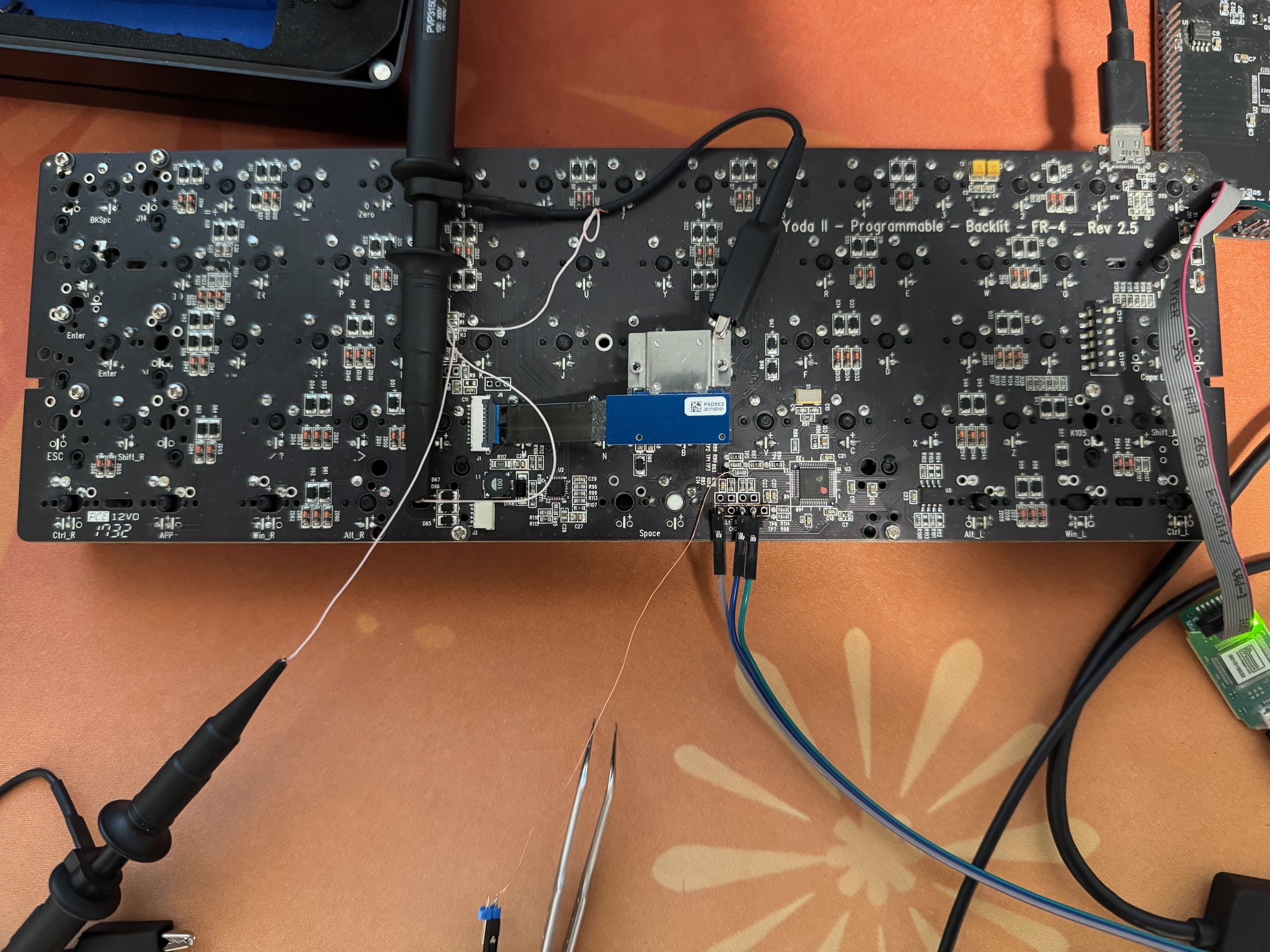
Now that we have figured out 5 (CLK, DATA, VCC ×2, GND) out of the 8 pins on our SN8 MCU, there are only 3 left. We then measured those three pins individually and realized they each have a one-to-one connection to the primary HT32 MCU. This greatly reduces the scope of the work we need to do analysis on. As shown in the previous post, we have managed to capture this communication between the SN8 and the HT32 controller. We strongly suspected it was I2C, but one thing we weren’t sure about is that the SN8 does not have native I2C support, and at the same time, those 3 pins are mapped to the hardware SPI peripheral. This led us down the road of trying to understand what kind of unusual uni-directional SPI we were looking at.
One new piece of information we captured this time: the clock is not very accurate, and it has timing skews that are highly correlated with when data transitions from 0 → 1. This is a strong indication that the clock is not driven by hardware, but rather bit-banged in software. It is not hard to imagine the code could look something like this:
for byte in bytes_to_send:
    for bit in byte.bits:
        if bit == 1:
            set_data_high()
        set_clk_high()
        slightly_longer_wait()
        set_clk_low()
        set_data_low()
And matching that up with our previous capture below,
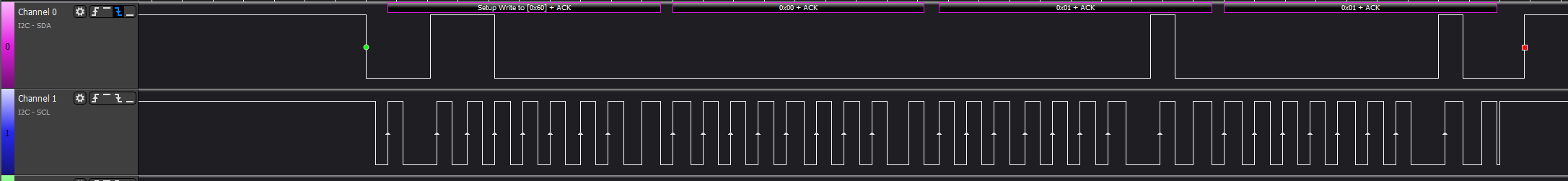
it makes perfect sense!
This finally confirmed that it is indeed I2C. The next step was to decode the actual protocol. Knowing that this message originated from a PS2 device,
naturally we assumed this would more or less represent the PS2 protocol itself.
And indeed, it does! Normally with PS2 mice, it would send a 3 byte packet for
each update, 1 byte of “flags” and 2 bytes of “X/Y” offset. The flags actually
contain 2 sign bits for the X/Y offset respectively. However, here as I move the
mouse left / right, up / down, I see the first byte always remains 0x00, while
the second and third byte alternates between positive and negative (starts with 0xFx)
values. So it sounds like the first byte is either unused or used only for mouse
button reporting (which we don’t have connected anyways), and the later 2 bytes
went from the standard unsigned value in PS2 to a signed 8 bit integer.
Validating our thoughts
Now that we have a good understanding of the communication protocol, it is time for us to write some code to validate our hypothesis.
As soon as we erased the primary controller, we noticed that nothing was being sent on the I2C (or even PS2) bus. We got a little scared, thinking we had broken something. Then we realized the trackpoint module was not being powered at all — there was no VCC!
This really puzzled us for a bit. For one, there was no obvious sign of anything
that looked like a MOSFET or DC-DC regulator (which would make no sense anyway,
since both the primary and secondary controllers run at 3.3V). Then, suddenly, we
noticed that on the far left side of the keyboard — far away from any of the MCUs —
sat a tiny “transistor” labeled Q10. When we probed it for continuity, one of its
legs was connected to the VCC line of both the trackpoint module and the SN8 MCU!
This was definitely the missing piece of the puzzle. Suddenly it all made sense:
the SN8 MCU has absolutely no dedicated reset pin. So the HT32 needs some way
to reset it, and cutting and restoring power (a power-on reset) is the simplest
possible solution!
After setting the PA10 pin on the HT32 MCU to low, we’ve enabled the MOSFET, and
power is applied to the trackpoint module as well as the SN8 MCU. This finally got
us seeing data again on the I2C bus!
One of the last things to do was to write a piece of sample code that can print out any data that’s “written” to this fake I2C device.
W 030 n=3 d=00 04 FB
W 030 n=3 d=00 05 FB
W 030 n=3 d=00 04 FD
As you can see from the data, the SN8 writes to I2C address 0x30 with 3 bytes of
data each time. And this perfectly matches what we’ve guessed earlier:
0x00 | Y Offset | X Offset.
Closing Thoughts
I think this series on documenting reversing this keyboard is probably coming to a close at this point. We have managed to resolve the communication protocol of this unknown controller via data analysis and reconnaissance. Thinking back, is this the only way we could’ve done this? Probably not, especially given one of the first steps was that we extracted a firmware image from the official firmware update tool. I’m sure given enough time and patience, especially with the help of AI, we could’ve figured all of this out from just the Main MCU’s code.
Honestly, this was a really fun exercise, and one of the most complex keyboards I’ve reverse engineered so far. I’m really looking forward to getting OpenOCD working for Holtek MCUs, as well as getting either RMK or QMK ported over to this keyboard.